
PIC Microcontroller Series — Part 2
PIC Microcontroller Series - 2
Under the hood of the PIC10F200. A deep dive into memory, the stack, registers, config bits, TRIS, OPTION, and dissecting the blink code line by line.
Under the Hood
PIC10F200 architecture explained
A deep dive into what makes your blink program actually work.
In Part 1, you got an LED blinking — but if you're like most beginners, you probably copied the code and trusted it would work. That's fine! But now let's pull back the curtain and understand why it works.
By the end of this post, you'll understand every line of that blink program and be ready to modify it confidently.
The PIC10F200's tiny brain
1. On-chip program memory — your code lives here
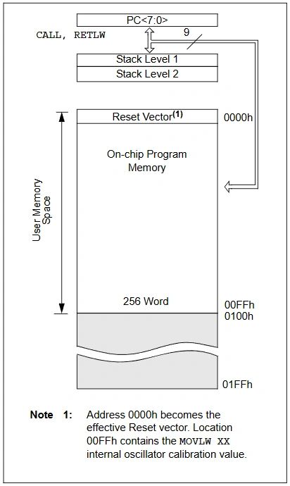
- Size: 256 words (512 bytes)
- What it stores: Your actual program instructions
- Quirk: Unlike most processors, your code doesn't start at address
0x000. Notice this comment in the code:

2. The stack — return address storage
- Size: Only 2 levels deep
- What this means: You can only nest subroutine calls 2 deep
- Practical impact: Keep your code structure simple
        call level1
      ; level1 calls level2
      ; level2 calls level3 ← STACK OVERFLOW!
In the stack overflow example above, the PIC10F200 would likely reset or behave unpredictably rather than gracefully handle stack overflow.
3. Data memory — variables and registers
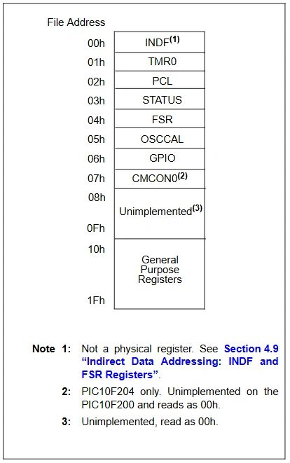
Only 16 bytes of user RAM!
The general-purpose registers are your variable storage space — where you store counters, temporary values, and any data your program needs to remember.
In the delay routine, we use registers 0x10h, 0x11h, and 0x12h as the outer, middle, and inner loop counter.
This means that we would still have 13 more bytes of usable RAM.
Dissecting your blink code line by line
Let's take apart that assembly blink program from Part 1.
Configuration bits explanation
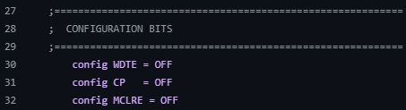
config WDTE = OFF — Watchdog Timer Disable
- What it is: A hardware timer that automatically resets the MCU if not periodically "fed"
- Why OFF: Your blink program runs in an infinite loop — the watchdog would reset the chip thinking it's stuck
- When you'd use it: In production code to recover from software crashes
config CP = OFF — Code Protection Disable
- What it is: Prevents reading/copying your program memory via programmer
- Why OFF: We want to be able to read back our code for debugging
- When you'd use it: In commercial products to protect intellectual property
config MCLRE = OFF — Master Clear Reset Enable Disable
- What it is: Makes
GP3/MCLRpin a reset input when enabled - Why OFF: We're not using external reset, and this gives us more flexibility with
GP3 - Effect:
GP3remains input-only but won't reset the chip when pulled low
Why this matters: These aren't just "boilerplate code" — they fundamentally change how your hardware behaves. For example:
WDTE = ONwould reset your LED every few secondsMCLRE = ONwould reset your program ifGP3went low
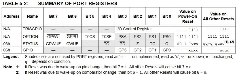
Configuring TRIS — the I/O control register

The first instruction movlw is move literal into the Working register. The Working register is the primary accumulator for data operations. Here we are moving the binary value 00001000 into the w register. The tris instruction configures the data direction of the GPIO pins — input or output. In this case, the tris is taking the bit mask loaded in the w register and setting it in the TRIS register. The GPIO part just tells the assembler "configure the TRIS register that corresponds to the GPIO port". We are not actually setting anything in the GPIO register yet.
Breaking down 0b00001000:
When setting up pin directions with the TRIS register, we use bits 0-3 where 1 = input and 0 = output. Then when controlling pin states with the GPIO register, we use the same bits 0-3 to set pins high (1) or low (0).
GP0= Output (Pin 7) — UnusedGP1= Output (Pin 6) — UnusedGP2= Output (Pin 5) — Your LED pin!GP3= Input (Pin 4) — Input-only pin
Key insights:
- TRIS register: Controls direction (input/output)
- GPIO register: Controls state (high/low)
GP3is input-only on the PIC10F200. You can't make it an output, which is why you will always see bit position 3 set to1(input).
Note: Pins 4-7 described above are the physical pin numbers on the 8-pin package, not GPIO bit numbers.
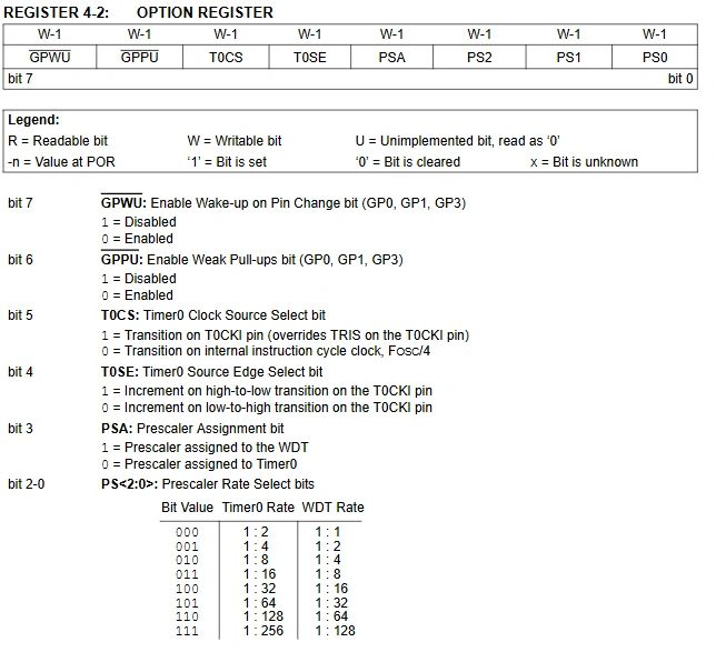
OPTION register — the control center

The code includes some more documentation of this critical register.
The configuration 0b11001000 (or 0xC8 hex) explained:
GPWU = 1— Disable wake-on-change (no sleep wakeups)GPPU = 1— Disable all weak pull-upsT0CS = 0— Timer0 uses internal instruction clock —GP2as digital outputT0SE = 0— Timer0 Source Edge Select bit — doesn't matter becauseT0CS = 0PSA = 1— Prescaler assigned to WDT (unused)PS2:PS0 = 000— Prescaler = 1:1 (unused)
What this configuration does:
- Ensures
GP2is NOTT0CKI - No pull-ups
- No wake-on-change
- Timer0 and WDT left unused
Critical point: T0CS = 0 ensures GP2 remains a normal GPIO pin. If this was 1, GP2 would become the Timer0 clock input and couldn't drive your LED!
LED control — set and clear
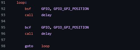
BSF vs BCF instructions:
bsf= Bit Set File: sets one bit to1bcf= Bit Clear File: clears one bit to0
What we are saying here is: set the bit (GPIO_GP2_POSITION) in the GPIO register to 1 (High/LED ON), call the delay, then clear the bit (GPIO_GP2_POSITION) to 0 in the GPIO register.
By using bit manipulation, you only affect the specific bit you want to change. This preserves other pins — GP0, GP1, GP3 remain unchanged.
Why not toggle? The PIC10F200 doesn't have a bit-toggle instruction, so you manually set and clear.
Note:
GPIO_GP2_POSITIONis a predefined constant fromxc.incwith value2(becauseGP2is bit 2 in the GPIO register). Alternative:GPIO, 2.
The delay routine
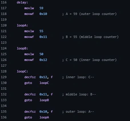
This isn't your typical beginner delay loop.
Understanding decfsz — the loop workhorse

What happens:
- Decrement: Subtract 1 from memory location
0x12 - Store: Put result back in
0x12(that's what,fmeans) - Test: If result is zero, skip the next instruction
- Continue: If not zero, execute the next instruction
Example:
- 1st time:
0x12goes from 50 to 49 (not zero, sogoto loopC) - 2nd time:
0x12goes from 49 to 48 (not zero, sogoto loopC) - …
- 50th time:
0x12goes from 1 to 0 (zero! so SKIP the goto and continue)
Alternative: decfsz 0x12, w would put the result in the W register instead.
Note: Remember that
0x10-0x1Fare general-purpose registers where we can store data.
Calculating the delay:
- Inner loop: 50 iterations × 3 cycles = 150 cycles
- Middle loop: 55 iterations × 150 cycles = 8,250 cycles
- Outer loop: 59 iterations × 8,250 cycles = 486,750 cycles
- Setup overhead: ~13,000 cycles
- Total: ~499,968 cycles
The PIC10F200 has a 4 MHz internal clock and an instruction cycle consists of four cycles. Basically, your instruction rate is 4 MHz / 4 = 1 MHz or 1,000,000 cycles where a single cycle is 1 μs (microsecond).
499,968 × 1 μs = 499.968 ms ≈ 500 ms
The padding trick — three ways to extend time
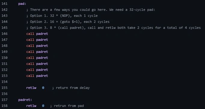
The code demonstrates something clever — precise cycle padding. You need exactly 32 cycles to reach 500,000 total cycles, and we show three different approaches.
Why the call/return approach is clever
Option 3 breakdown:
call padret= 2 cycles (push return address, jump topadret)retlw 0= 2 cycles (pop return address, return)- Total per call: 4 cycles
- 8 calls: 8 × 4 = 32 cycles exactly!
Advantages of this approach:
- Fewer lines: 8 calls vs 16 gotos vs 32 NOPs
- Demonstrates subroutines: shows call/return mechanism
- Easy to count: 8 × 4 = 32
- Reusable:
padretcould be used elsewhere if needed
What retlw 0 does:
- Return: Pop the return address from the 2-level stack
- Literal: Put the value
0in theWregister - Why
0?: The return value isn't used, so0is conventional
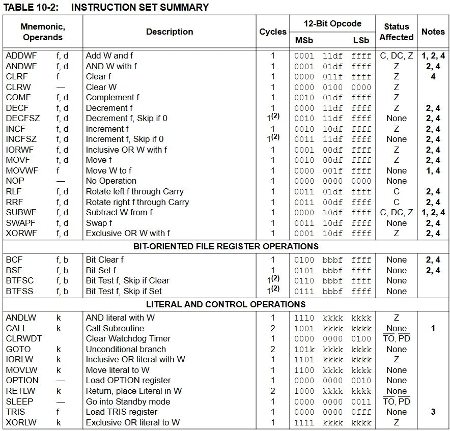
Full instruction set
Takeaways
Your new blink program demonstrates several advanced concepts:
- Precise timing calculation (500 ms exactly)
- Proper documentation (bit-level register explanations)
- Modern toolchain usage (
pic-aswith custom linker options) - Memory-efficient variable usage (
0x10-0x12allocation)
This isn't just "make LED blink" — it's a foundation for understanding embedded timing and control. More information about this microcontroller, including the datasheet and other supporting collateral, can be found on Microchip's website: PIC10F200 | Microchip Technology.
Coming up in Part 3
We'll add button input and explore debouncing, building on this solid architectural understanding.
Related project
Comments
Comments are powered by Giscus + GitHub Discussions. Enable them by filling in siteConfig.comments in src/lib/config.ts.