PIC Microcontroller Series — Part 5
PIC Microcontroller Series - 5
Retro gaming meets modern embedded: read an NES controller with a PIC16F1455 and drive 8 LEDs through a CD4094B shift register. Serial protocols, PLL clocks, rrf, rlf, comf, and register banking.
Retro Gaming Meets Modern Embedded: NES Controller and Shift Registers
The big upgrade: from simple to sophisticated
We've reached an exciting milestone in our PIC journey! After mastering the basics with the PIC10F200, it's time to graduate to a significantly more capable microcontroller and tackle a project that bridges retro gaming with modern embedded systems.
What you'll learn:
- Upgrading to the PIC16F1455 with enhanced capabilities
- Serial communication protocols (NES controller reading)
- Hardware expansion using shift registers
- Multi-input/multi-output system design
- Real-time input processing and response
GitHub code: nes_with_shift_register.s
Datasheets:
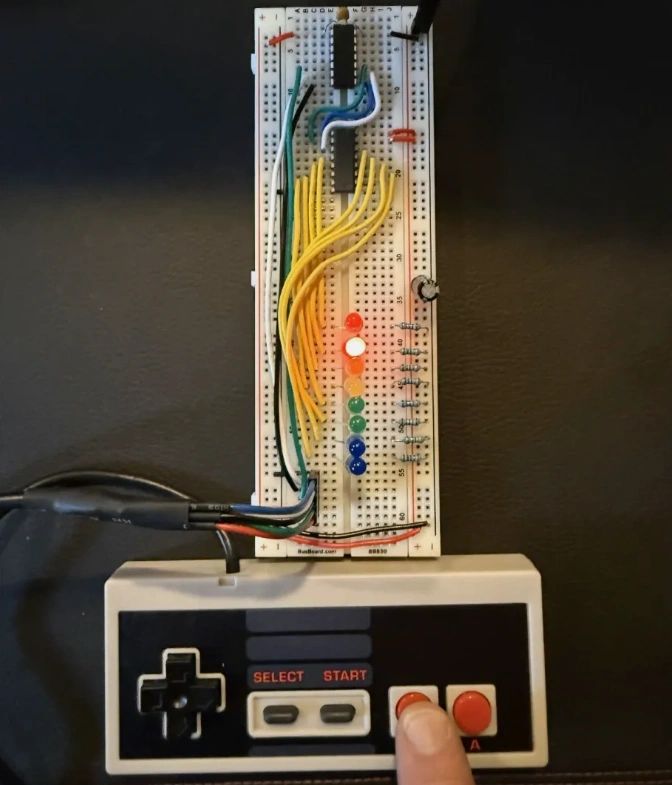
Hardware end result
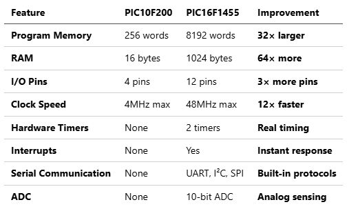
The hardware leap: PIC10F200 vs PIC16F1455
Why we're upgrading
The PIC10F200 served us well for learning fundamentals, but it has serious limitations.
Note: Remember that in PIC terminology, "words" refers to program memory locations that store instructions. Each "word" holds one assembly instruction (14 bits on the PIC16F series). So 8,192 words = 8,192 individual assembly instructions that can be stored in program memory.
PIC16F1455: a modern 8-bit powerhouse
The PIC16F1455 represents a major step up, moving from the 8-pin PIC10F200 to a more capable 14-pin package.
Enhanced features:
- Phase-Locked Loop (PLL): Multiply internal clock for higher speeds
- Advanced oscillator control: Precise timing and frequency management
- Multiple clock sources: Internal, external, USB clock generation
- Enhanced GPIO: More pins with advanced configuration options
- Brown-out reset: Automatic reset during power fluctuations
- Low-voltage programming: Easier development and debugging
Project overview: NES controller interface
Input side: NES controller (4021 shift register)
- 8 digital buttons: A, B, Select, Start, Up, Down, Left, Right
- Serial protocol: Clock, latch, and data communication
- Nintendo-standard interface: Works with any authentic NES controller
Processing: PIC16F1455 microcontroller
- High-speed operation: 48 MHz with 3× PLL multiplier
- Real-time response: Process all 8 buttons in microseconds
- Protocol management: Handle both input and output serial communication
Output side: CD4094BE shift register + 8 LEDs
- I/O expansion: Control 8 LEDs using only 3 microcontroller pins
- Visual feedback: Each button press lights its corresponding LED
- Instant response: No perceptible delay between press and illumination
Why this project matters
This isn't just about reading game controllers — it demonstrates fundamental embedded systems concepts:
- Serial communication: Understanding how devices exchange data efficiently
- Hardware expansion: Multiplying I/O capability through clever design
- Real-time systems: Processing inputs fast enough for human interaction
- Protocol implementation: Following established communication standards
- Retro interface: Connecting modern microcontrollers to classic hardware
Hardware deep dive: understanding the components
NES controller internals: the 4021 shift register
Inside every NES controller is a CD4021BE 8-bit shift register that converts parallel button states into serial data.
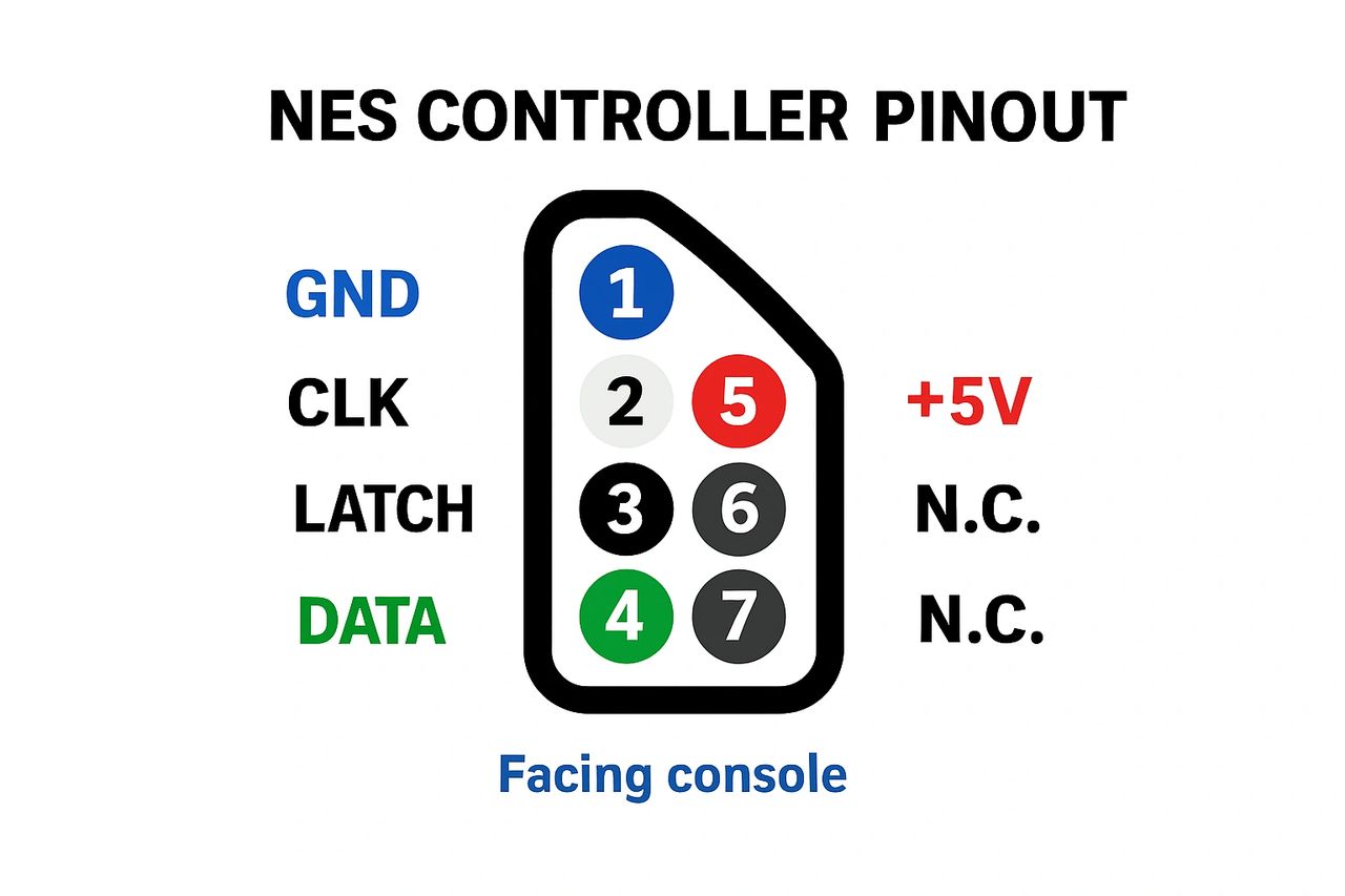
Note: The colors represented here are from the particular controller I was using at the time from an NES clone. Yours may be different, but the pinout will be the same.
The NES communication protocol:
- Latch pulse (12 μs): Captures current button states into shift register
- 8 clock cycles: Shift out one button state per clock pulse
- Data reading: Read data line on each clock's falling edge
- Button order: A, B, Select, Start, Up, Down, Left, Right
CD4094BE output shift register
For LED control, we use a CD4094BE 8-bit shift register with latch.
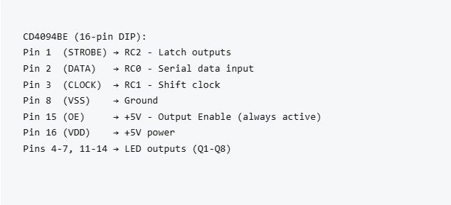
Key features:
- Serial input: Receive data one bit at a time (MSB first)
- Parallel output: Drive 8 LEDs simultaneously
- Latched outputs: Store data internally, update all outputs at once
- 3-wire control: Data, clock, and strobe (latch) signals
PIC16F1455 pin assignment
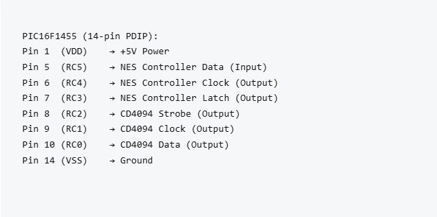
Note: We're using
PORTCexclusively — all 6 pins for our serial communication needs.
Serial communication protocols explained
Understanding serial vs. parallel communication
Parallel communication (like our early LED examples):
- One wire per bit: 8 bits needs 8 wires
- Simultaneous transfer: All bits sent at once
- Fast but expensive: Requires many pins
Serial communication (like NES controller):
- One data wire: All bits sent sequentially
- Clock synchronization: Separate clock wire coordinates timing
- Efficient: Fewer wires, more complex protocol
NES controller protocol timing
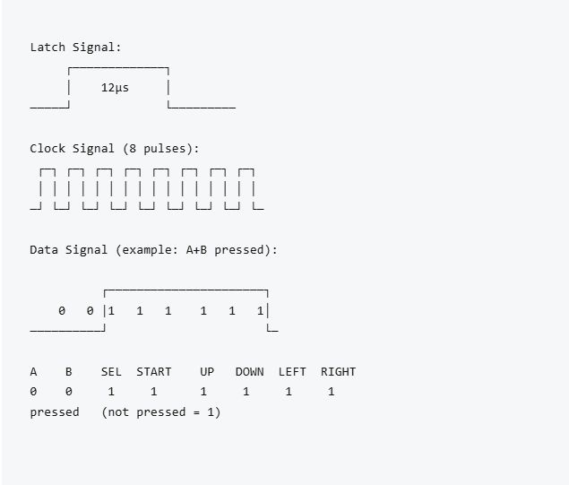
This was difficult to show in ASCII format, but I wanted to provide a visual representation of what it looks like when you press buttons.
One "pulse" = one complete clock cycle (high + low).
So when we say "8 pulses," it means:
- 8 complete cycles
- Each cycle has a HIGH portion and a LOW portion
- Data is typically read on either the rising edge or falling edge
For the NES controller specifically, the data is read on the falling edge of each clock pulse (when the clock goes from HIGH to LOW). Each complete clock cycle transmits one bit of button data.
CD4094 shift-register protocol
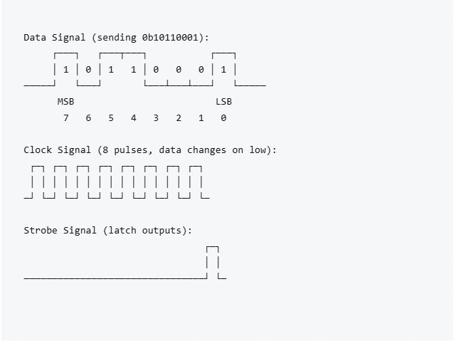
The CD4094 shift register receives data MSB first (Most Significant Bit first), which is the opposite of how the NES controller sends data.
Understanding MSB vs LSB:
- MSB (Most Significant Bit): The leftmost bit (bit 7) with the highest value (128)
- LSB (Least Significant Bit): The rightmost bit (bit 0) with the lowest value (1)
- MSB first: Send bit 7, then bit 6, then bit 5… down to bit 0
- LSB first: Send bit 0, then bit 1, then bit 2… up to bit 7
CD4094 data processing:
- Serial input: Data enters one bit at a time on each clock pulse
- Internal shifting: Each new bit pushes previous bits deeper into the register
- MSB-first order: First bit sent becomes the final MSB of the stored byte
- Parallel output: After 8 clocks, all outputs reflect the complete byte
Example with 0b10110001:
- Send order: 1 (bit 7), 0 (bit 6), 1 (bit 5), 1 (bit 4), 0 (bit 3), 0 (bit 2), 0 (bit 1), 1 (bit 0)
- Final result: Q7=1, Q6=0, Q5=1, Q4=1, Q3=0, Q2=0, Q1=0, Q0=1
Note: Q0-Q7 are the output pins of the CD4094. Q7 is the highest bit output pin, Q0 is the lowest bit output pin. Each Q output connects to an LED in our circuit.
Code analysis: advanced assembly programming
Let's examine our program and understand the techniques used.
Enhanced configuration: PLL and clock management
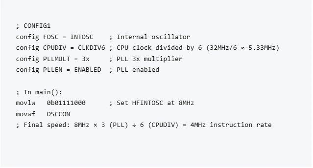
Understanding the clock configuration:
- Internal oscillator: 8 MHz high-frequency internal oscillator
- PLL multiplier: 8 MHz × 3 = 24 MHz
- CPU divider: 24 MHz ÷ 6 = 4 MHz instruction rate
- Why this setup: Fast enough for responsive communication, slow enough for precise timing
GPIO initialization: all-digital configuration
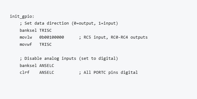
Key differences from PIC10F200:
- Banking: Must select correct register bank before access
- ANSELC register: Explicitly disable analog functions (ADC)
- More control: Separate control over each pin's analog/digital mode
NES controller reading: precision serial communication
Step 1: Latch button states
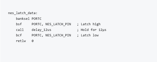
What happens: The 12 μs pulse tells the NES controller's internal 4021 shift register to "capture" the current state of all 8 buttons into its internal storage.
Step 2: Clock out 8 button states
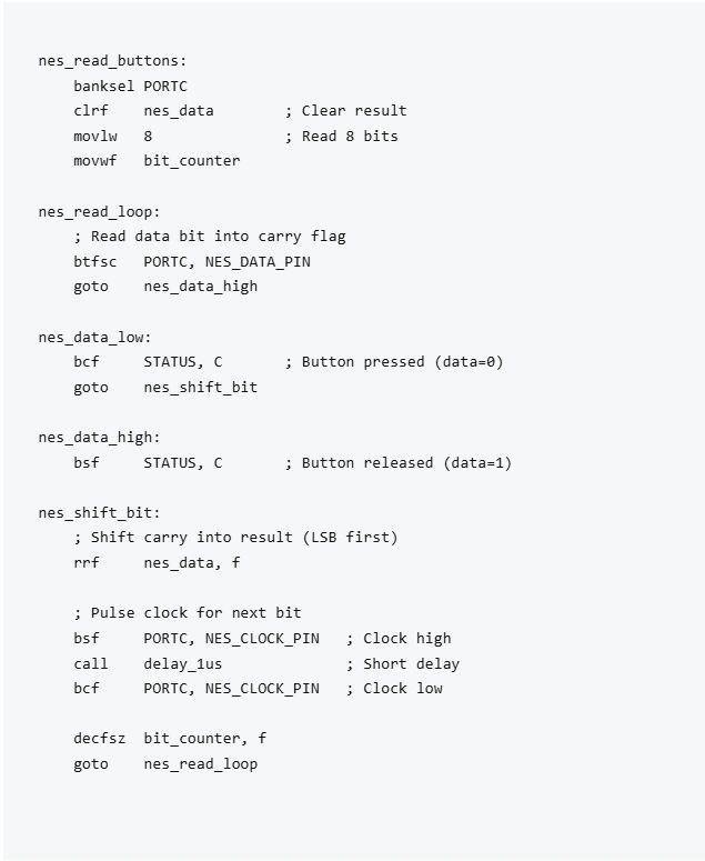
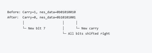
Advanced technique: Using the carry flag as temporary storage for each bit, then shifting it into the result with rrf (Rotate Right through File).
New instruction: rrf — Rotate Right through File
rrf nes_data, f
What rrf does:
- Shifts all bits right: Bit 7 → 6, Bit 6 → 5, etc.
- Carry → Bit 7: Carry flag becomes the new MSB
- Bit 0 → Carry: LSB shifts into carry flag
- Result stored in file: The
fdestination stores result back
Example:
Why this is perfect for NES reading:
- Carry holds new bit: From our button reading
- Shifts into position: Builds result bit by bit
- Automatic ordering: Creates proper button sequence
Data inversion: pressed = 1 for LEDs
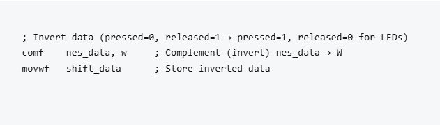
Why invert?
- NES logic: Pressed button =
0, Released =1(active-low) - LED logic: We want pressed button to turn ON LED (=
1) - Solution:
comf(complement file) inverts all bits
Note: I chose inversion because I like the visual representation with all LEDs being OFF and only turning ON when a button is pushed. Otherwise, all LEDs would be ON and turn OFF on button push, which would consume more power needlessly for this project.
New instruction: comf — Complement File
comf nes_data, w
What comf does:
- Inverts every bit: 0 becomes 1, 1 becomes 0
- Bitwise NOT operation:
~(input) - Example:
0b01010010 → 0b10101101
Shift register output: sending LED data
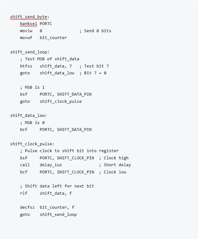
Key points:
- MSB first: CD4094 expects most significant bit first (opposite of NES reading)
- Bit testing:
btfss shift_data, 7tests the MSB directly - Left rotation:
rlfshifts data left to present next MSB
New instruction: rlf — Rotate Left through File
rlf shift_data, f
What rlf does:
- Shifts all bits left: Bit 0 → 1, Bit 1 → 2, etc.
- Carry → Bit 0: Carry flag becomes new LSB
- Bit 7 → Carry: MSB shifts into carry flag
- Result stored in file: Updates the original register
Perfect for serial transmission:
- Presents MSB: Bit 7 always holds the next bit to send
- Automatic shifting: Each
rlfpresents the next bit - No complex indexing: Simple loop sends all 8 bits
Output latching: updating all LEDs simultaneously
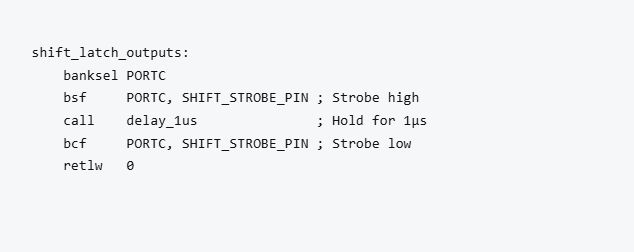
Why latching matters:
- Internal storage: Shift register stores data internally during shifting
- Simultaneous update: Strobe pulse updates all 8 outputs at once
- No flicker: Users see instant, clean transitions (not progressive shifting)
Register banking in PIC16F1455
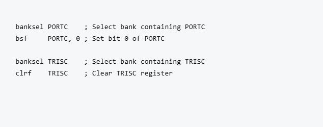
Unlike the simple PIC10F200, the PIC16F1455 has multiple register banks to access its expanded feature set.
Why banking is needed:
- Limited address space: 8-bit addresses can only access 256 locations
- More registers: PIC16F1455 has many more control registers
- Bank switching:
bankselgenerates the code to switch register banks
Precision timing at higher speeds
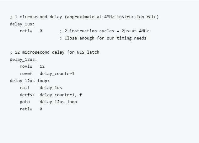
Timing requirements:
- NES latch: 12 μs minimum pulse width
- Clock periods: 1 μs between clock edges
- Setup/hold: Data must be stable when clock changes
Program flow: real-time processing loop
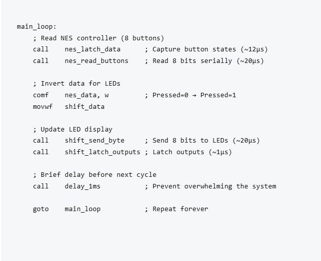
Total processing time: ~53 μs per complete cycle. Update rate: ~1000 Hz (with 1 ms delay). Response time: < 1 ms from button press to LED illumination.
Why this speed matters
Human perception:
- Visual lag threshold: ~20 ms (50 Hz) before humans notice delay
- Gaming response: < 10 ms feels instant
- Our system: < 1 ms = virtually instantaneous response
Technical benefits:
- Real-time feel: No perceptible delay between input and output
- Smooth operation: Fast enough for responsive gaming
- Overhead available: 99% of CPU time available for expansion
Advanced microcontroller features
- PLL clock multiplication for higher performance
- Register banking for accessing expanded features
- Precision timing for protocol compliance
- Multi-pin coordination for complex I/O operations
Serial communication expertise:
- Protocol implementation following exact specifications
- Bit-level data manipulation using carry flag and rotation
- Bidirectional communication managing input and output simultaneously
- Real-time constraints meeting timing requirements reliably
System design principles
Hardware expansion:
- I/O multiplexing using shift registers for pin efficiency
- Component selection matching microcontroller capabilities to requirements
- Interface standardization maintaining compatibility with existing hardware
Software architecture:
- Modular design organizing complex functionality into manageable pieces
- Real-time programming balancing multiple timing-critical operations
- Resource efficiency minimizing memory and processing overhead
Embedded systems concepts
This project demonstrates several key embedded systems principles:
- Real-time response: The system must process inputs and update outputs fast enough that users perceive instant response. Our <1 ms latency achieves this goal.
- Protocol compliance: Embedded systems often must interface with existing hardware using established protocols. Following NES timing specifications exactly ensures compatibility.
- Resource optimization: Using shift registers to expand I/O capability shows how clever hardware design can overcome microcontroller limitations efficiently.
- Modular programming: Breaking complex operations into focused subroutines creates maintainable, debuggable code that can be easily modified or expanded.
What's next: Part 6 preview
The ultimate upgrade: We've mastered serial communication and retro interfaces, now it's time for the grand finale!
In Part 6, we'll make one final massive leap to the PIC32MX170F256B — a 32-bit MIPS processor — and build a complete Space Invaders style arcade game.
The big jump:
- Architecture: 16-bit → 32-bit MIPS processor
- Programming: Assembly → C language with XC32 compiler
- Memory: 1 KB RAM → 64 KB RAM + 256 KB Flash
- Clock speed: 48 MHz → 48 MHz with advanced PLL control
- Display: 8 LEDs → 128×64 pixel OLED graphics
- Communication: Basic serial → I²C protocol implementation
What we'll explore:
- 32-bit programming: C language development on MIPS architecture
- Graphics programming: Bitmap rendering and sprite-based graphics
- I²C communication: Advanced serial protocol for display control
- Real-time gaming: 60 FPS gameplay with collision detection
- Persistent storage: EEPROM high-score saving
- Professional game design: Complete game with levels, difficulty scaling, and polish
The complete Space Invaders game:
- OLED graphics: 128×64 pixel monochrome display showing crisp game visuals
- Smooth gameplay: Player movement, bullet shooting, enemy spawning
- Progressive difficulty: Enemy speed and spawn rate increase with score
- Collision detection: Precise hit detection between bullets and enemies
- High-score system: Persistent storage using EEPROM
- Professional polish: Game-over screens, level indicators, smooth animations
Advanced embedded concepts:
- Memory management: Efficiently using 64 KB RAM for game objects
- Real-time systems: Maintaining 60 FPS while processing game logic
- Hardware abstraction: Clean separation between game logic and hardware
- Modular architecture: Professional code organization and design patterns
From simple LED blinkers to a complete arcade game — this series takes you from basic embedded programming to complete interactive systems!
This project proves that embedded programming can be both technically sophisticated and genuinely fun. By connecting classic gaming hardware to modern microcontrollers, we've demonstrated that the principles of good embedded design — timing, efficiency, modularity, and real-time response — can create engaging interactive experiences.
The NES controller interface serves as a foundation for countless projects: from simple LED displays to complex gaming systems. Most importantly, it shows how understanding both hardware protocols and software implementation can bridge decades of technology evolution.
This is Part 5 of our PIC Microcontroller Series. Master these serial communication concepts to unlock advanced embedded system capabilities.
Related project
Comments
Comments are powered by Giscus + GitHub Discussions. Enable them by filling in siteConfig.comments in src/lib/config.ts.